ML20NB50AE
POWER MOSFET WAFER DATASHEET
Feature
- 20V N-Channel MOSFET High Dense Design.
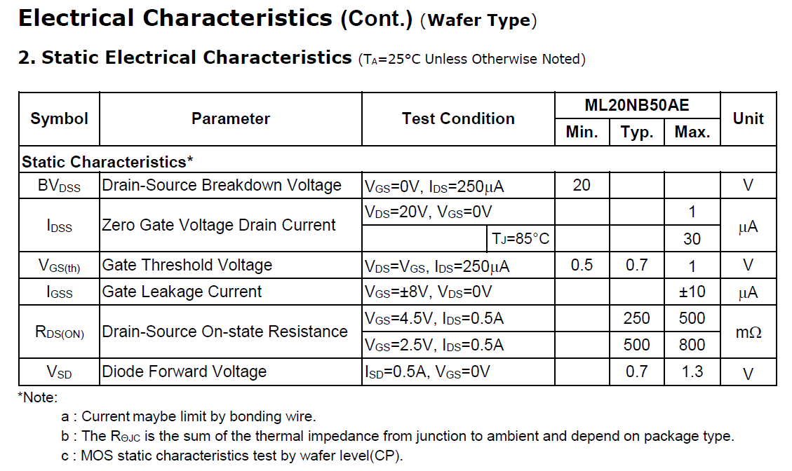
- RDS(ON) =250mΩ(typ.) @ VGS= 4.5V
- RDS(ON) =500mΩ(typ.) @ VGS= 2.5V
- Reliable and Rugged
- ESD Protected up to 2KV
Applications
- Portable Equipment and Battery Power Systems
Die Description

- Wafer Diameter: 8 inchs. (±0.1inches)
- Wafer Thickness: 6mils. (±0.6mils)
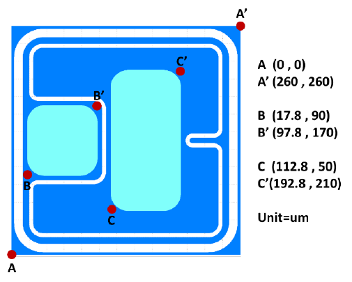
- Die Size: 320μm × 320μm.(Including scribe line)
- Scribe Line Width: 60μm.
- Metalization: Frontside:Al/Si/Cu , Backside:Ti/Ni/Ag.
- Metal Thickness:
Frontside:4μm , Backside:1.4μm.
- Bonding Area:
Gate:80μm × 80μm.
Source: Full metalized surface of source region
- Recommended Wire Bounding
Gate: 1milx1 Cu
Source: 1milx2 Cu
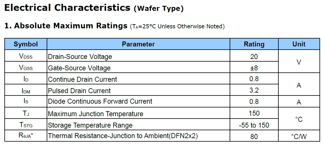
Electrical Characteristics I
Electrical Characteristics II


